 LWDAQ Driver (A2071) Design and Development

© 2011-2021 Kevan Hashemi, Brandeis University© 2022-2026 Kevan Hashemi, Open Source Instruments Inc.
Note: All our schematics and Gerber files are distributed under the GNU General Public License.
[15-MAY-24] Here are the various design files for our A2071A and A2071E assemblies.
S2071_1: Controller and Relay[10-MAY-18] The A2071A built with the A207102A printed circuit board requires a wire link from !RESET to !SYSRST and the track from !SYSRST to P6 must be cut. This allows the !RESET signal to reset the ring oscillator and registers in the P2071A firmware. Boards modified in this way have hardware version zero, HV=0. The A2071A build with the A207102B printed circuit board require no modifications and have hardware version one, HV=1.
The A2071E built with the A207101A/B printed circuit board has hardware version number zero, HV=0. These boards do not provide protection against an out-of-range voltage being returned from a faulty device, so U17 is in danger of over-heating. Furthermore, they have trouble reading out a camera over a 120-m cable because their pull-up and pull-down resistors are 1 kΩ instead of 10 kΩ.
The A2071E made with the A207101C printed circuit board provides protection resistors R117 and R118. If its pull-up and pull-down resistors are 1 kΩ, it still cannot read a camera out over a 120-m cable. Its hardware version is one, HV=1.
The A2071E made with the A207101C/D printed circuit board, with 10-kΩ pull-up and pull down resistors has hardware version two, HV=2.
[17-JUN-13] The A2071E with an LM6172M in place of U17 is vulnerable to a device setting R+ or R− outside the range 0..+3.9 V. For example, if the device wires R+ to +15 V, U17 will find its output shorted to 3.3 V through diode array U31. The op-amp overheats, breaks, and starts to bring down the ±15 V power supply. In the A207101C layout, we add 1 kΩ resistors R117 and R118 between the outputs of U17 and the U31 diode clamps. This modification is difficult on the A207101B circuit board, and would itself compromise the reliability of the circuit. We decide to leave the A2071Es that exist now as they are. They will be hardware version 0.
[07-AUG-13] We repair two broken A2071Es. In one, some problem with one of the DG411DY analog switches was pulling R+ and R− down to −4 V when we selected an empty driver socket. When combined with our problem with taking R+/R− outside the range −0.6-4.1 V, U17 was over-heating and dying. We replaced DG411DYs and U17 and board works fine. The other had a damaged U20. Neither fault appears to have originated because of the lack of R117 and R118 on the V0 hardware.
[29-JAN-14] Two months ago we received 5 A2071Es with V1 hardware, which includes R117 and R118. We omit R12 so as to indicate to the firmware the hardware is version one.
[03-APR-15] We find that the A2071E with V1 hardware won't read out a camera over a 120-m cable, while the A2037E does so with no problem. We replace the 1 kΩ resistors R14 and R15 with 10 kΩ, to mimic the A2037E pull-up and pull-down resistors. Now the A2071E reads out over 120 m. We present these observations in more detail here. We change the value of resistors R14, R15, R17, R18, R20, R21, R23, R24, R26, R27, R29, R30, R32, R33, R35, and R36 to 10 kΩ. This is the V2 hardware. We set up V2 by loading R12 (sets bit zero to zero) and omitting R13 (sets bit one to one).
[29-MAR-16] We have Q0213 returned from Genova, Italy. They reported that it was over-heating and shutting down. We open the case and see L1 is discolored. We apply power and after ten minutes, L1 and U8 are too hot to keep a finger on, but 3.3 V power is still present. The driver is still functional. The RCM6700 is hot also. We remove it from the board. After five minutes, L1 and U8 have cooled down. We connect 24-V power from a bench-top supply. Driver Q0213 draws 350 mA with the RCM6700 plugged in, and 190 mA without the RCM6700. Driver Q0142 draws 210 mA and 120 mA respectively. Driver Q0244 draws 350 mA and 190 mA respectively, then the 3.3-V power supply fails completely and the circuit draws 120 mA. Driver Q0245 draws 210 mA at 24 V without opening the box. It appears that our ASD05-12S3 converters are faulty. We have already decided to replace the ASD05-12S with the PYB10-Q24-S3. We will add to quality control a measurement of the driver 24-V input current consumption in future. We replace the ASD05-12S3 on Q0213 and Q0244. They now draw 190 mA for one second after applying 24 V, and 220 mA afterwards, when the RCM6700 module comes out of reset.
[30-MAR-16] We note excessive ground noise on the metal enclosure of a device plugged into driver Q0245, which is still equipped with the ASD05-12S3 converter.
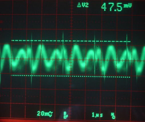
We switch to Q0244, which has the PYB10-Q24-S3 converter, and obtain the following noise. The 24-V power supply to the driver remains the same.

The spikes drop from around 60 mVpp to 30 mVpp, while the harmonic pattern drops from 50 mVpp to 20 mVpp. We replace the ASD05-12S2 on drivers Q0244, Q0245, Q0213, and Q0142.
[19-AUG-16] We study the reception of serial bytes by the controller from LWDAQ devices. The bytes are marked by a 50-ns LO start bit, the eight data bits, each 50 ns, most significant to least significant, then a return to HI for at least 100 ns before the next transmission. The controller uses two versions of the serial logic signal TXI. One is TXIS, which is clocked by CK, the 40-MHz clock, and the other is TXIF, which is clocked by FCK, the 80-MHz clock. The state machine that receives the bytes is itself clocked by CK, and leaves its rest state when it detects a LO on TXIS. The first rising edge of CK discovers the LO. The second moves the receiver into state 1. The third moves it to state 2. The fourth rising edge clocks the value of TXIF into a shift register as the first serial bit. The rising edge of FCK occurs roughly 2 ns before the rising edge of CK. The question arises: will this timing give reliable reception for all phases of CK, for small variations in clock frequency, for reasonable jitter in the clock?
The Serialization.tcl program is a Toolmaker script that simulates variation in clock phase with random jitter and any number of serial bits. We can vary the delay between the time at which we sample TXI and the time of the rising CK edge that clocks the sample into the shift register.
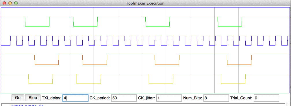
We find reception for eight bits is reliable with jitter ±0.5 ns, clock period 25.0 ns, and delay 0-25 ns. Our delay is 2 ns, which is on the edge of the reliable window. We would do better to sample TXI with the falling edge of CK, which would give us a delay of 12.5 ns, in the center of the window. With a 12.5 ns delay, we can tolerate clock jitter of ±2.5 ns, or period range 25±0.5 ns. Given the proven reliability of the existing firmware, however, we deem it unwise to attempt an improvement to the de-serializer.
[29-JUN-17] We have firmware P2071A01.abl for the A2071A running with VME read and write time 160 ns from DS to DTACK. The top orange indicator is Board Select, meaning the address on the VME backplane selects the A2071A. The second orange indicator is Activity, meaning VME reads and writes are taking place.
[26-JAN-23] We receive back from Fermilab S0199, D0616, and C0009 all with the same symptoms, plus their power supplies and a cable that we believe is the cause of the damage to these three drivers. We start with C0009. Component U22, ADS8505, is damaged. It does not assert its BUSY line. The controller uses the ADS8505 conversion delay for timing, so it gets stuck. The Diagnostic acquisition stalls because it uses the converter delay, while BCAM acquisition does not stall but returns black images. We replace the ADS8505. We now get a Diagnostic Instrument report of power supplies, but we still see black images in the BCAM Instrument. Component U23, ADS828E, is damaged. We replace U23 and now the board passes all tests. We check all connections on the suspect cable, including looking for all possible shorts between conductors. We find nothing wrong. We inspect the jacket for breaks and find only abrasion from dragging, but no breaks. We open up S0199 and observe the same symptoms. But D0616 has different symptoms: Diagnosic Instrument acquisition succeeds, but the power supply voltages appear to be zero when they are in fact turned on. We see black images from the BCAM Instrument. Component U23, ADS828E, is hot. On all three boards, we observe RB, the bottom reference voltage produced by U23, to be around 0.2 V when it should be around 2.0 V. Remove ADS828E on D0616 and find the ADS8505 is also faulty. The faulty ADS828E upsets voltages CM and RB. But the input V8 is clamped by U24 to −0.7V to +5.7 V. The voltage V16 cannot go outside ±15V, while the ADS8505 is tolerant of ±25 V. Hypothesis: the cable connected +15V to +5V. The controller's +5V exceeded +6 V. The only devices that require +5V to be less than +6V are the ADCs.
[02-JUN-23] We are preparing to assemble five more A2071E. We update the BOM to eliminate the scarce ZVN3306, replacing it with the DMN67D7L.
[03-JUL-24] We note that some of the newer RCM6700 modules cause our A2071E to reset every second or so for ten or twenty seconds before stabilizing. It turns out that the boot-up power consumption of the cold RCM6700 is sufficient to overwhelm our 3.3-V power supply, dropping its voltage from 3.3V to 3.0V, which causes the MCP130T-315I to generate a reset. We order the same part with 3.00 V and 2.70 V reset points. We change the part called for by the A2071E BOM to the 3.00 V part for now.
[08-JUL-24] We load MCB130T-300 instead of MCP130T-315I for our power supply supervisor. We do not see the boot-up reset problem with this new, lower-threshold device. We update the A2071E and A2071A bills of materials.
[15-JAN-26] We have 8 of A2071A from Tufts and CERN. We plug into a VME crate along with A2087 TCP/IP interface Boards X00025, X00033, X00035, X00037, and X00053 pass all tests. We burn in X00037 and X00053 for an hour with a BCAM and set aside for return to CERN. Board X00040 ±15V and +5V converters won't power up. Remove U22 and U23, no change. Remove converters and power with external ±15V. Component U27, DG407, pops and smokes. Remove U27, normal current drawn. Restore converters, powers up fine. In crate, sometimes responds with version numbers, sometimes does not. Sometimes powers up, sometimes does not. Board X00024 the +5V power was not coming up. Replaced DC-DC converter, now get +5V. Wash and put in oven to dry. Check X00038, power supplies won't come up but responds to VME.