 Input-Output Head (A2057) Manual
© 2004, Mike Bradshaw, Brandeis University© 2008-2020, Kevan Hashemi, Brandeis University
© 2025, Kevan Hashemi, Open Source Instruments Inc.
| Description |
| Connectors |
| Command Bits |
| Analog Inputs |
| Digital Outputs |
| Analog Outputs |
| Software |
| Obsolete Versions |
| Design |
| Development |
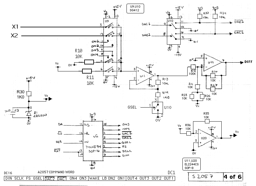
[12-DEC-25] The Input-Output Head (A2057) is a LWDAQ device that provides two analog inputs, two analog outputs, and four open-drain digital outputs. We can read the analog inputs and set the logic outputs with the LWDAQ Voltmeter Instrument. The A2057's analog outputs are provided by two eight-bit, serial, digital-to-analog converters (DACs). To set the output voltages of the DACs, we transmit a sequence of commands, as detailed below. The Voltmeter Instrument does not provide a button that sets the DAC voltags.
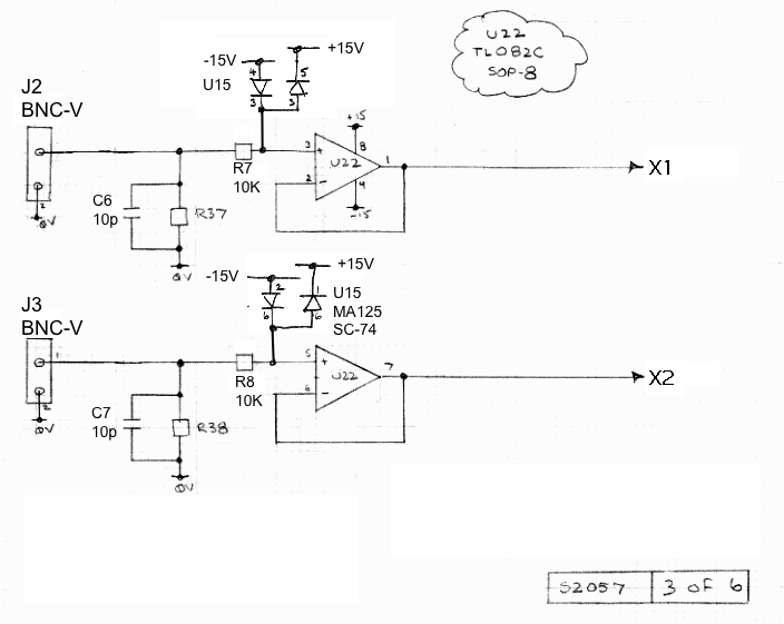
Vertical BNC sockets J2 and J3 provide connection to an oscilloscope probe or a coaxial cable. The default input impedance at the socket is 1.0 MΩ in parallel with 10 pF, as is standard for an oscilloscope input. Between the input and its buffer amplifiers are a 10 kΩ resistor and diode clamps that limit the input voltage to ±15 V. The dynamic range of the inputs is ±10 V, but they can tolerate ±500 V. We may add simple filter to each input circuit by cutting a track on the top side of the board. These tracks are boxed on the silk screen and labelled X1 and X2. Having cut the track, the left pad will present the input signal and the right pad is the continuation to the default input circuit. A 30-MΩ resistor between the X1 pads, for example, will provide a ÷31 divider and allow us to measure ±310 V on X1.
Digital outputs are presented on four-way plug P1. These we can either connect to zero with a transistor or leave high-impedance. Each transistor provides a diode that conducts when the digital output drops below −0.7 V. The maximum voltage on a digital output when high-impedance is 30 V. To accompany the digital outputs we provide a 0-V connection on all four corner mounting holes, as well as on P2-2 and P2-4.
| Version | Input Impedance |
X1 Range (min) |
X2 Range (min) |
Y1 Range | Y2 Range | Comments |
|---|---|---|---|---|---|---|
| A3036B | 1.0 MΩ | ±10 V | ±10 V | −10 to 9.6 V | −10 to 9.6 V | Red A205701H PCB. |
| A3036H | 32 MΩ | ±320 V | ±320 V | −10 to 9.6 V | −10 to 9.6 V | Red A205701H PCB with resistors added. |
| A3036R | 50 Ω | −60 to +20 dBm | −60 to +0 dBm | −10 to 9.6 V | −10 to 9.6 V | Red A205701H PCB with diode and LT5534 added. |
Analog outputs are presented on a four-way plug P2. They are 0-10 V voltages generated by an op-amp with a 1-kΩ series resistor. They will tolerate a short circuit indefinitely. We set the output voltages with a string of LWDAQ commands that write an eight-bit value to one of the two on-board DACs.
The A2057 connects its 0V potential to its four mounting holes. But it does not connect the shield of its LWDAQ socket to the 0V potential. The LWDAQ grounding rules prohibit a connection between the 0V potential and the shield, in order that we may avoid ground loops in large experiments. As a LWDAQ device, the A2057 is designed to wake up and take measurements, then go back to sleep. In the awake state, the circuits internal ±15 V analog power supplies are turned on. But in the sleep state, they are turned off. The digital outputs do not use the ±15 V power suppliess. They are powered by the 3.3 V logic supply, which never turns off. The digital outputs will persist when the A2057 is asleep. When we measure input voltages, we wake up the board, measure the voltages, and put the board to sleep again. When we use the analog outputs, however, we must not send the board to sleep after configuring the outputs, or else the analog output amplifiers will lose power. The Voltmeter Instruments daq_no_sleep option leaves the A2057H awake between measurements. The analog outputs will be unaffected by voltage measurements.
[20-FEB-20] The two four-way plugs P1 and P2 are 0.1" pitch headers with gold-plated pins a single back-wall locking latch (such as Molex 0022112042). To mate with these connectors, we use crimp terminal (such as Molex 0008550102) in a four-way housing (such as Molex 0022013047). Pin one of each plug is on the left when the locking latch is to the rear, and is also marked by a square pad visible on the bottom side of the board. The signals on P1 and P2 are marked on the silk screen.
| Pin | Function |
| 1 | Y1, Analog Output 1 |
| 2 | 0V, Connected to Mounting Holes |
| 3 | Y2, Analog Output 2 |
| 4 | 0V, Connected to Mounting Holes |
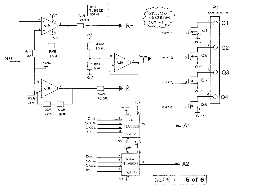
Each pin on P2 is the drain of an NDS355AN mosfet. The outputs Q1..Q4 are controlled by device command bits DC1 to DC4 (OUT1 to OUT4).
| Pin | Function |
| 1 | Q1, Digital Output 1, MOSFET Drain |
| 2 | Q2, Digital Output 2, MOSFET Drain |
| 3 | Q3, Digital Output 3, MOSFET Drain |
| 4 | Q4, Digital Output 4, MOSFET Drain |
When DCn is HI, the MOSFET of Qn turns on, connecting Qn to 0 V through a resistance of approximately 0.2 Ω. When the command bit is LO, the mosfet is off and Qn is open circuit, except for the clamping diode that turns on when Qn drops below −0.7 V.
The table below gives the assignment of LWDAQ command bits to the A2057 functions.
| DC16 | DC15 | DC14 | DC13 | DC12 | DC11 | DC10 | DC9 | DC8 | DC7 | DC6 | DC5 | DC4 | DC3 | DC2 | DC1 |
|---|---|---|---|---|---|---|---|---|---|---|---|---|---|---|---|
| DIN | SCLK | FS | GSEL | DAC2 | DAC1 | ON4 | ON3 | WAKE | LB | ON2 | ON1 | OUT4 | OUT3 | OUT2 | OUT1 |
To determine the command word that will implement a particular operation on the A2057, write out sixteen bits in a row, starting with bit sixteen (DC16) on the left, and ending with bit one (DC1) on the right. Set each bit to zero or one as you require. The left-most four bits form the most significant nibble of the sixteen-bit command word. The right-most four bits are the least significant nibble. Translate each nibble into a hex digit, and you have the hex version of the command word.
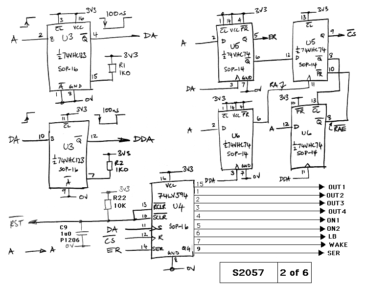
The A2057 provides four analog input channels. We set one and only one of the ON1..ON4 bits to select one and only one of the four analog inputs for amplification and transmission back to the LWDAQ Driver. In the LWDAQ Driver, this input is available to for 16-bit analog to digital conversion. The A2057's two analog inputs are selected by bits ON1 and ON2. The ON3 and ON4 channels are connected to 0V and 5V respectively, and allow the Voltmeter Instrument to auto-calibrate the A2057.
The A2057 provides two amplifier gains, one of which is eleven times higher than the other. We call them the ×1 and ×11. The GSEL bit, when set, selects the higher gain. With ×1 gain, the dynamic range of the two analog inputs is ±15 V. With ×11 gain, the range is ±1.5 V.
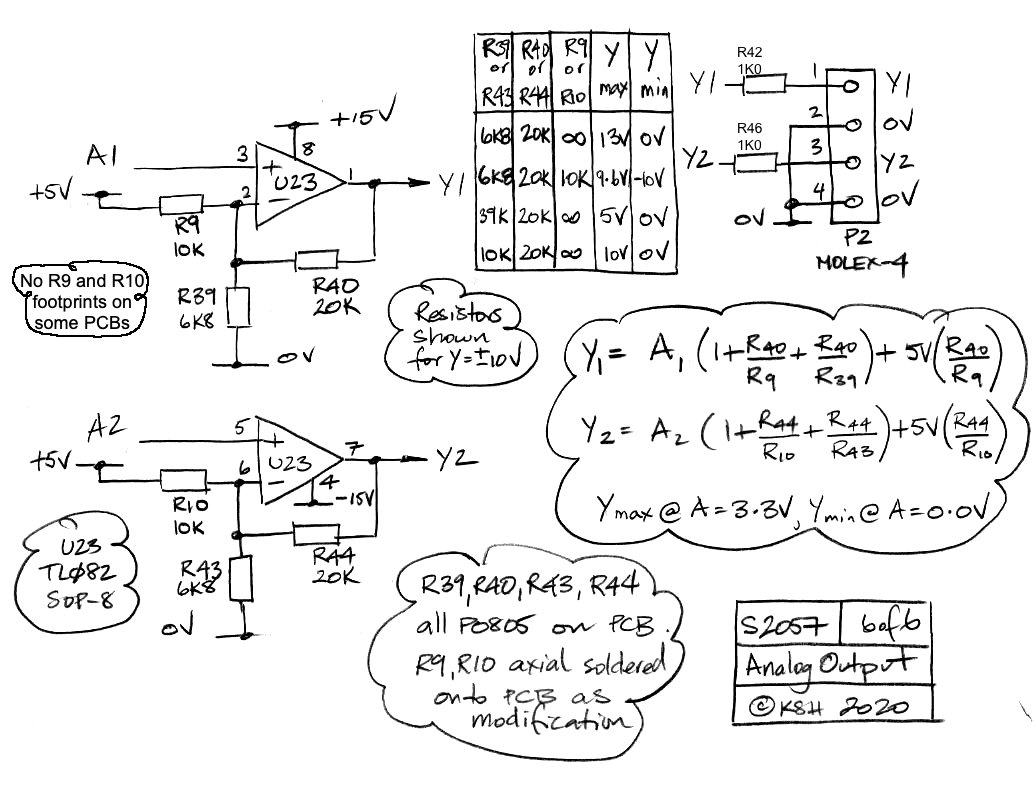
The A2057 uses two Texas Instrument's TLV5623 8-bit digital-to-analog converters. The output of each DAC is passed through an adjustable op-amp gain stage.
The A2057 uses four NDS355AN n-channel mosfets. When OUTn is asserted, signal Qn will be connected to 0 V through one of these mosfets. When OUTn is unasserted, OUTn will be open-circuit.
[29-SEP-25] The A2057 provides two analog inputs on J2 and J3, which are BNC connectors and are set up for use with ×10 oscilloscope probes. For existing software to read the analog inputs, see above. Here we describe how to select the analog inputs with LWDAQ command words. To select analog input n we set bit ONn and clear the other three ON bits. We set GSEL if we want ×11 gain. We set WAKE to provide power to the amplifiers. We clear LB because we do not want the LVDS transmitter to assert a logic level on the R lines. We must set the OUT1..OUT4 bits to be consistent with the desired state of these four digtal outputs Q1..Q4. If we are not using them, then we can clear them all. But if we want them to remain in the same state, we must set them to the same values we used in the previous command word we sent to the A2057.
Once we have transmitted a command word, the A2057 asserts an analog voltage on the R signal back to the LWDAQ Driver. There we can digitize the voltage with LWDAQ driver commands. The following commands select analog input number one and digitize it 100 times with the sixteen-bit ADC in the LWDAQ Driver, leaving the 100 samples stored in the first 200 bytes of the driver memory. The samples are spaced by 8000 "delay ticks", each of which is 125 ns for a 1 kSPS sample rate. The driver job number "11" is the 16-bit ADC convert and store job.
LWDAQ_transmit_command_hex $sock "0090"
LWDAQ_set_repeat_counter $sock 99
LWDAQ_set_delay_ticks $sock 8000
LWDAQ_execute_job $sock 11
The voltage returned to the LWDAQ Driver is linear with respect to the voltage applied to the A2057 input. We can determine the input voltage from the driver voltage if we have an intercept and slope. We obtain the intercept and slope by reading input channels three and four (ON3 and ON4), which provide us with a known 0-V and 5-V input at the A2057. The Voltmeter Instrument uses these reference inputs to auto-calibrate the voltage it reads from the A2057. You will find the above steps implemented with Tcl in Voltmeter.tcl and our Tool script A2057_Tester.
[20-FEB-20] The four digital outputs are set by the four independent OUT1..OUT4 bits in the command word. When one of these bits is set, its corresponding digital output pin on connector P1 will be connected to 0V by an NDS355AN transistor. The channel resistance of this transistor with a 3.3-V gate voltage is around 0.2 Ω. When the OUT bit is clear, the transistor is turned off, so the output pin is open-circuit. The outputs are "open-drain". If we connect them to +15V with a 10-kΩ resistor, we will see +15 V on the output pin when the OUT bit is clear, and 0 V when the bit is set. We can use these mosfets to turn on relays and lamps, but note that they include a diode between the drain and source, which prevents the output pin from dropping below −0.7 V.
Warning: The analog outputs are disabled when we send the A2057 to sleep. In the Voltmeter Instrument, use daq_no_sleep = 1 to keep the board awake.
[20-FEB-20] The A2057 analog outputs are provided by two eight-bit serial DACs. The DAC outputs are amplified and buffered by two op-amps. The analog outputs are presented on connector P2 as described above. The Voltemeter Instrument does not allow us to set the analog outputs. Instead, we must send a sequence of commands to the A2057 to configure one of its 8-bit DACs. These commands control the DAC serial data input and serial clock directly, and so clock in a new sixteen-bit DAC word, of which eight bits dictate the analog output from the TLV5623 eight-bit DAC. Do not confuse the 16-bit LWDAQ command with the 16-bit DAC control word. We use a sequence of LWDAQ commands to send a single DAC control word. The Set Voltage script is an example Toolmaker script that allows us to set the analog outputs. You can run it with Run Tool from the LWDAQ Tool menu.
The first four bits of the DAC's sixteen-bit control word are control bits. The next eight bits are the DAC value. The final four bits are all zeroes. The A2057 uses six command bits to control the DACs. These bits are DIN (DC16), SCLK (DC15), FS (DC14), DAC2 (DC12), DAC1 (DC11), and WAKE (DC8). The DAC1 and DAC2 bits select which DAC to use. We can assert one or both, to select one or both DACs. The DAC1 and DAC2 signals are effective only when FS is asserted. The WAKE bit must be asserted to provide power to the A2057. The FS, or frame synchronize, must be asserted once at the beginning of each data word transfer, and once again at the end of each data word transfer. The DIN, or data input, bit is the serial data bit that delivers DAC instruction. The falling edge of SCLK clocks DIN into the selected DACs.
A sixteen-bit control transmission to a DAC requires a total of thirty-five command transmissions, which takes at least 140 μs, not counting the time taken for TCPIP communication between the data acquisition system and the LWDAQ driver. The maximum square-wave output frequency of the DACs is 3.5 kHz. The list below gives an example command word sequence that sends one control word to DAC1. The DAC integer value we send in this example is 170, or binary 10101010. We give the LWDAQ commands as hex values. The most significant nibble pulses SCLK, and the last three nibbles stay the same for a given DAC. Some of the bits in the sixteen-bit serial word are not used by the DAC, so we give them the name "X" and set them to zero. We use "0x" to mean "hexadecimal".
Most of the command bits are not in use during this procedure, as is plain from the table. The figure below shows the same progression, but makes clearer how the DAC data bits change on the rising edge of SLCK, so that they can be established and valid when the DAC reads them on the falling edge of SCLK. Neither DAC will be altered unless we assert FS.
The routine below performs the above operation for us, for any decimal value 0..255, by making contact with a driver, selecting the A2057 device, and constructing and transmitting the thirty-five commands.
#
# A2057_set_dac takes a driver IP address, ip, a driver socket number, dsock,
# a multiplexer socket number, msock, a dac number, dac, and an eight-bit dac
# value in decimal, value, and these to set an A2057 dac value. The routine
# opens a socket, selects the A2057 and sends a string of thirty-five commands
# to the device to set one of its DAC outputs.
#
proc A2057_set_dac {ip dsock msock dac value} {

	# Construct the sixteen bit value we must send to the DAC.
	if {![string is integer -strict $value]} {
		error "value \"$value\" not an integer."
	}
	if {($value>255) || ($value<0)} {
		error "value \"$value\" must be 0..255."
	}
	set bits 0000[LWDAQ_decimal_to_binary $value 8]0000

	# Open a socket to the driver and select the A2057.
	set sock [LWDAQ_socket_open $ip]
	LWDAQ_set_driver_mux $sock $dsock $msock

	# Assert the frame sync bit.
	LWDAQ_transmit_command_hex $sock "6C80"

	# Select DAC1 or DAC2.
	if {$dac == 1} {set c "480"} else {set c "880"}
	LWDAQ_transmit_command_hex $sock "6$c"

	# Transmit sixteen bits. Each bit requires two command words, one
	# to present the bit value and raise the clock, another to continue
	# the bit value while dropping the clock.
	for {set i 0} {$i < [string length $bits]} {incr i} {
		set b [string index $bits $i]
		if {$b} {
			LWDAQ_transmit_command_hex $sock "C$c"
			LWDAQ_transmit_command_hex $sock "8$c"
		} else {
			LWDAQ_transmit_command_hex $sock "4$c"
			LWDAQ_transmit_command_hex $sock "0$c"
		}
	}

	# End the transmission by deselecting both DACs.
	LWDAQ_transmit_command_hex $sock "4080"

	# Close the socket to the driver, freeing it for other activity.
	LWDAQ_wait_for_driver $sock
	LWDAQ_socket_close $sock
}
The DAC outputs feed into their own adjustable-gain, adjustable-offset amplifier. By default, the A2057H amplifier takes the 0..3.3 V output of the DAC and amplifies it to 0..13 V. By choosing amplifier resistor values, we can provide alternate ranges and offsets, such as −10..+9.6 V, according to the equations found on schematic page S2057_6.
[20-FEB-20] We control and read out all versions of the A2057 with the LWDAQ Software. We read out the A2057 analog inputs with the software's Voltmeter Instrument. The same instrument allows us to set the digital outputs, but not the analog outputs. We can set the analog outputs wit the A2057_Tester.tcl, which is a LWDAQ Tool script, or with Set_Voltage.tcl, which is a Toolmaker script. You will also find routines to set the analog outputs in the Fiber Positioner Tool of the LWDAQ distribution, available in the Tool manu, with the source code in the LWDAW/Tools folder. You will find the data acquisition steps required to control and read out the A2057 in Voltmeter.tcl, which is the TclTk script that defines the Voltmeter Instrument. In Driver.tcl you will find the routines that compose TCPIP messages to communicate with a LWDAQ Driver.
[29-SEP-25] The history of the A2057 is confused by errors in the circuit diagram, since corrected, errors in labeling printed circuit boards, and un-recorded modifications to the circuit. In February 2020 we retired all previous versions of the circuit to make way for the A2057H. In 2025 we added the A3057R combined RF power meter and voltmeter.
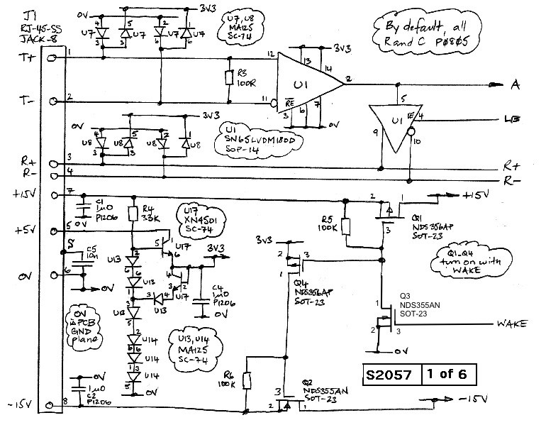
The A2057A provides three 4-way plugs for the inputs and outputs, as well as a grid of holes for additional circuits and connectors. The J2 connector accepts two analog inputs, J3 provides two analog outputs, and J4 provides four digital outputs. Despite being named J1..J3, these connectors are plugs, not sockets.
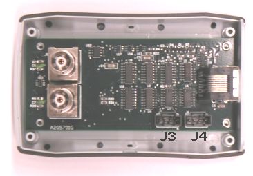
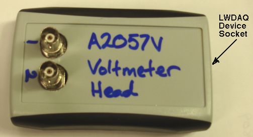
The A2057V comes in a PPL enclosure. It provides two BNC plugs for the two analog inputs, allowing them to be used with oscilloscope probes. The LWDAQ device socket is set in the end wall opposite the BNC connectors. Two 4-way plugs provide four digital outputs (J4) and two analog outputs (J3). The enclosure as shown does not give external access to the digital or analog outputs, but is easy to cut additional holes in the cover.
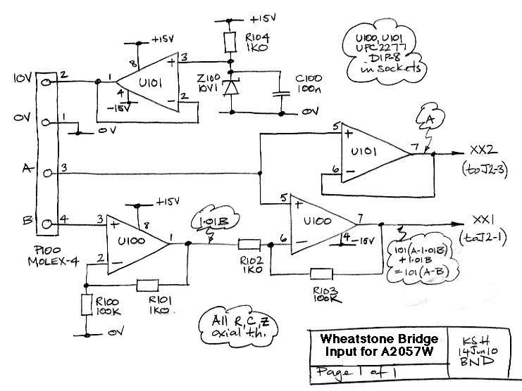
The Wheatstone Bridge Head (A2057W) adds a differential amplifier to the front end of the A2057A, as well as a 10-V power supply, as shown in S2057W_1. The A2057W allows us to power and read out most Wheatstone Bridge sensors. We connect the sensor to the new J100 plug, which provides 10-V power and accepts a differential input A/B from the bridge.
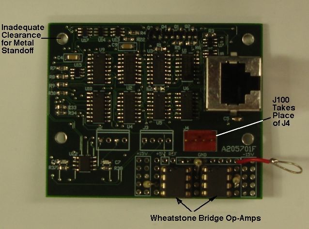
In the A2057W implementation shown above, we cut traces to J4 and put J100 in its place. All differential amplifier parts are installed on the patch area provided by the circuit board. Note that the A205701F circuit board, used by the A2057W, does not leave adequate clearance for metal standoffs in its top-left corner. There are several vias that will make contact with a hex nut on the top side of the board.
The A2057W is built on the A205701F circuit board. We cut the traces to J4 and use the J4 footprint for the four-way J100 connector.
| Pin | Function |
| 1 | 0V |
| 2 | 10V |
| 3 | A |
| 4 | B |
The Wheatstone Bridge amplifier circuit has inputs A and B and produces an output 101×(A−B). This output is called XX1 and connects to J2-1, where it is buffered and becomes X1, the first analog input of the A2057. Another output from the amplifier is A itself, which connects to J2-3, and so becomes X2.
[29-SEP-25] All our schematics and Gerber files are distributed under the GNU General Public License.
[19-FEB-20] Submit A205701H with red silk screen and HASL finish for fabrication on a five-day turn.
[23-FEB-22] Set R40 and R44 to 20 kΩ in two existing assemblies, modify to others, and we have four A2057H assembled with 31 MΩ input impedance on X1 and X2, providing a ÷32 attenuition for measuring ±320 V. Fiber_Positioner v1.3 working, an improved Set_Voltage.tcl that generates square waves.
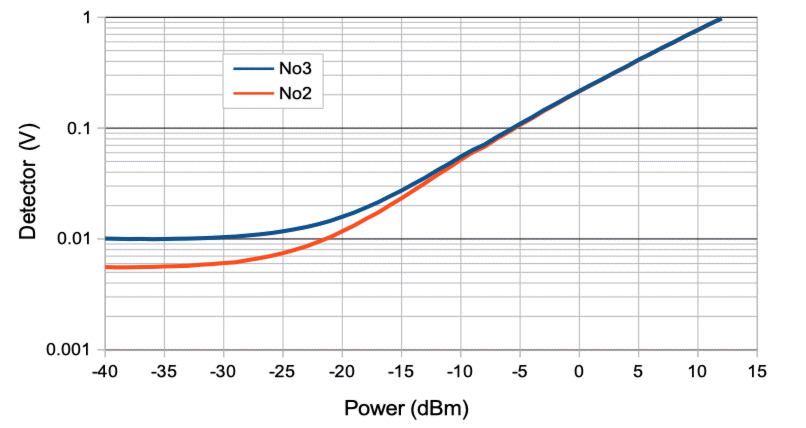
[29-SEP-25] We introduce a zero-bias diode radio-frequency (RF) power meter to X1 on two A3057 assemblies No2 and No3. We terminate X1 directly with 51 Ω. We take an SMS7630-006 zero-bias detector diode in SOT-23 package. We cut the X1 input trace and place one of the two diodes in our SOT-23 package in series with the input, so that the anode is connected to X1 and the cathode is connected to the amplifier. We add a 100 pF capacitor from the cathode to ground. We now have an RF to DC voltage converter. The following plot shows how the voltage recorded from X1 varies with RF power at 915 MHz.
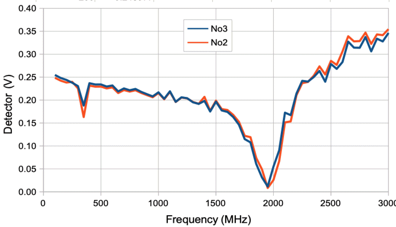
We set the RF power to 0 dBm and increase the frequency from 100 MHz to 3000 MHz. We are delivering the RF power to the X1 input BNC socket through a 1-m RG-58C cable. The power detector works well from 100 MHz to 1.5 GHz, but at higher frequencies our detector diode ground is inadequate. Attenuators on the X1 BNC socket, and varying the length of the cable through which we deliver the RF power did nothing to stop the dead spot at 2 GHz, nor the climb in detector voltage up to 3 GHz.
We use the detector diode input on the No2 assembly to measure the insertion loss of five 915-MHz ISM band filters. Two are ZX75BP-915-S+ from Minicircuits, three are CBPFS-0915 from Crystek. The ZX75BP filters have their SMA socket marked OUT and the plug marked IN. We measure the response of one of these filters in the forward and backward directions, to compare, and we see that the pass-band is sharper in the forward direction.
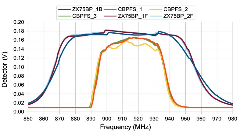
The calibration of this A2057R power detector is 216 mV at 0 dBm, 165 mV at −2 dBm, and 145 mV at −3 dBm. The pass-band insertion loss of all three filters is less than 3 dBm. The CBPFS filters attenuate to 20 mV within 10 MHz of their nominal 902-928 MHz passband. This 20 mV corresponds to −18 dBm.
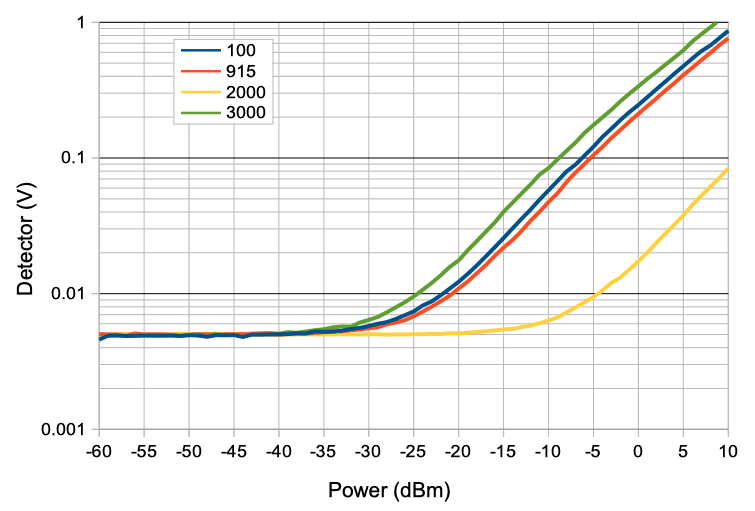
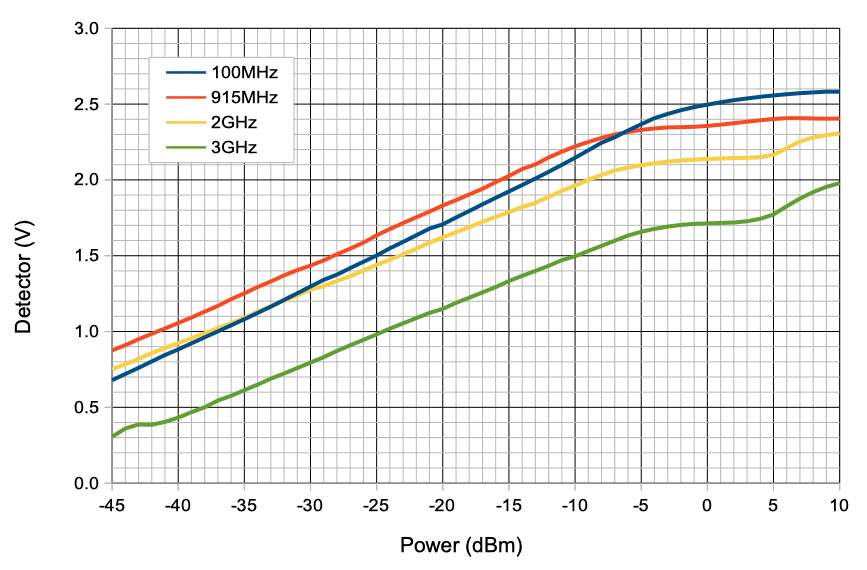
[30-SEP-25] We plot detector diode voltage of our No2 circuit versus power for four different frequencies.
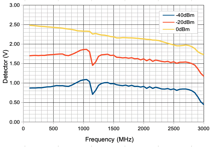
On our No2 circuit on the X2 input, we insert an LT5534. We load the SOT-363 package onto a six-pin SIP adaptor and solder to the breadboard area next to X2. We have a 51-Ω termination soldered directly to the BNC socket beneath the board. For power we use the local 3.3 V from one side of C4. We have 100 pF decoupling the power supply at the SIP-6 pins. We bring the RF signal in through 1.0 nF. The output of the chip goes directly to the X2 input.
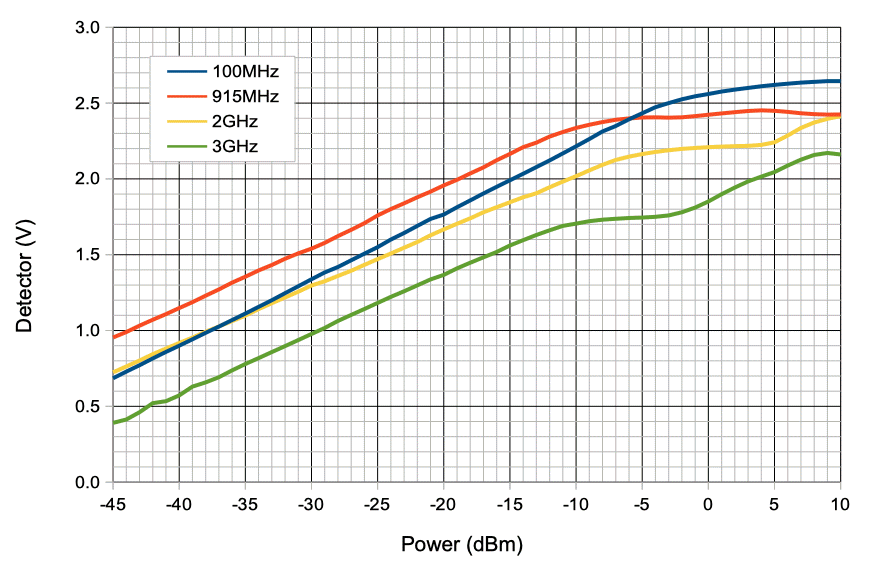
We vary frequency and measure the detector output for a selection of different power levels.
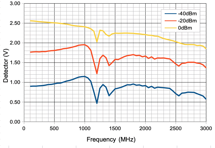
We make another LT5534 detector on No3 circuit X2 input. This time we load the 100 pF decoupling capacitor on the SIP-6, as well as some of the wire links.
Both our No2 and No3 circuits have input offsets around -3.0 V. We load 160 kΩ and 390 kΩ in parallel with R35, after which the offsets are 0 V and −1 V. We name this new A3057 version the A3057R.